The process of chip production is like constructing a house with lego, with wafers as the foundation, and then layers of chip production strategies on top of each other to provide the vital ic chips. However, with out the design, it’s miles vain to have a robust production potential, so the position of the architect is quite essential. But who are the architects in ic layout? The next a part of this paper is to introduce the ic design.
Inside the ic manufacturing method, ic is normally planned and designed by means of expert ic layout companies, which includes mediatek, qualcomm, intel and different well-known factories, all design their very own ic chips, providing distinct specs and performance chips to downstream manufacturers to select. Due to the fact the ic is designed by means of the manufacturing facility itself, the ic layout is very depending on the technology of the engineer, the first-class of the engineer impacts the value of an corporation. However what precisely are the stairs that engineers undergo while designing an ic chip?
Design the first step, set goals
In ic layout, the most essential step is the specification. This step is like finding out how many rooms, toilets, and building codes you need to follow before you layout a building, and then designing it after all of the features have been determined so you don’t must spend extra time making adjustments. Ic layout also wishes to go through a comparable step to make sure that the layout of the chip will not have any errors.
Step one within the system of specs is to determine the motive and overall performance of the ic, and set the general route. The next step is to see what protocols to conform with, inclusive of wireless card chips need to conform with ieee 802.11 and different specifications, in any other case, the chip will not be well suited with the product available on the market, making it not able to connect to other devices. Finally, it’s far to set up the implementation approach of this ic, assign exceptional features into unique units, and establish the link approach among specific units, in order to finish the system of specifications.
After designing the specs, it is time to layout the information of the chip. This step is like taking down the preliminary plans of the building, drawing out the overall outline for later drawing. In ic chips, hardware description language (hdl) is used to explain the circuit. The generally used hdl has verilog, vhdl, etc., thru the program code can effortlessly express the feature of an ic. The subsequent step is to test the correctness of this system’s functionality and preserve to alter it till it meets the favored functionality.
With computer systems, the whole thing is less difficult
With the whole plan, the next step is to attract the layout blueprint of the aircraft. In ic layout, the logical synthesis step is to determine the precise hdl code, placed it into the electronic layout automation device (eda device), and allow the laptop convert the hdl code into a common sense circuit, resulting in the following circuit diagram. Then, again and again determine whether or not the common sense gate layout meets the specifications and regulate till the characteristic is correct.
Subsequently, the synthesized code is positioned into another set of eda tools for circuit format and winding (location and route). After continuous trying out, the following circuit diagram will be shaped. Inside the photograph, you may see exceptional colorations which includes blue, pink, inexperienced and yellow, and every exclusive shade represents a light mask. The way to use the mild masks?
Layer on pinnacle of every different with a chip
First, it’s miles now known that an ic produces a couple of mask, that have top and decrease layers, and every layer has its own task. The following is a simple instance of a mask, taking cmos, the most basic component in integrated circuits, as an instance. Cmos stands for complementary metal-oxide-semiconductor (complementary steel-oxide – semiconductor), which mixes nmos and pmos. Shape cmos. As for what is a metal oxide semiconductor (mos)? This extensively used thing inside the chip is more difficult to explain, the general reader is also more tough to apprehend, here will not be extra specific.
Inside the discern beneath, the left is the circuit diagram shaped after the circuit layout and winding, and it’s far recognised in the front that each shade represents a light masks. At the proper is how each mask is unfold out. Production is, begin from the bottom, follow the approach stated in the preceding ic chip production, make layer via layer, and ultimately produce the preferred chip.
At this factor, the ic design ought to have a initial understanding, the general appears very clean ic layout is a totally complex expert, however additionally way to the adulthood of laptop-aided software program, in order that ic design can be extended. Ic layout manufacturing unit may be very dependent on the intelligence of engineers, every step described right here has its very own specialised understanding, may be impartial into a number of professional courses, together with writing hardware description language isn’t always best need to be acquainted with the programming language, it is also necessary to apprehend how the logic circuit works, a way to convert the desired set of rules right into a software, and how the synthesis software converts the program into a logic gate.
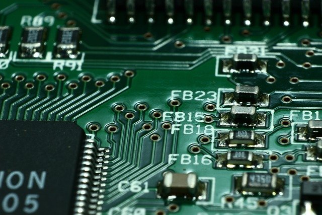
After expertise that ic designers are like architects, and wafer foundries are building factories, it’s time to understand a way to finally bundle the chip into a glance acquainted to the common consumer, this is, a “bundle.”
Let you know what is encapsulation
After a protracted technique, from layout to production, ultimately got an ic chip. However, a chip is pretty small and thin, and may be without problems damaged by way of scratches if it isn’t always covered externally. Further, due to the small length of the chip, it will now not be easy to manually deploy at the board without a bigger housing. Therefore, the rest of this newsletter describes encapsulation.
At gift, there are two types of not unusual applications, one is the dip package deal not unusual in electric powered toys, which is black and looks like a centipede, and the alternative is the gba bundle commonplace when buying a boded cpu. As for other packaging strategies, there are pga (pin grid array; pin grid array, or dip’s advanced model of qfp (plastic square flat bundle). Because there are so many packaging strategies, the following could be an creation to dip and gba packaging.
Conventional packaging, enduring
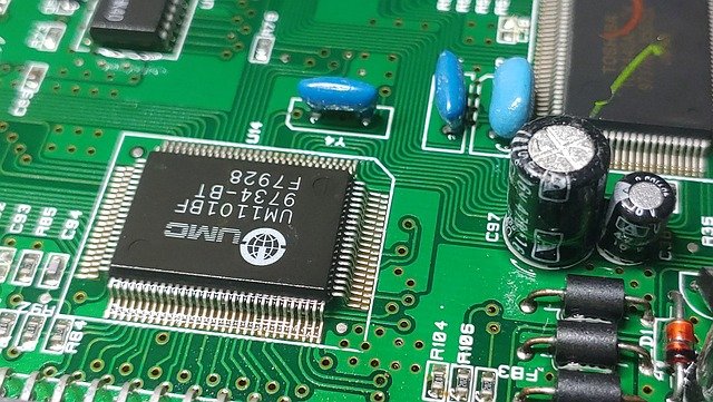
Initially, we have to introduce the twin inline package (dip). As may be visible from the following determine, the ic chip the usage of this bundle looks like a black centipede on the foot of the dual inline bundle, which is stunning. This packaging technique is the earliest ic packaging technology adopted, and has the benefit of low cost. Suitable for small chips that do not require too many wires. But, due to the fact maximum of them are plastic, the warmth dissipation effect is poor, and it cannot meet the requirements of modern-day excessive-speed chips. Consequently, most of the chips that use this bundle are long-lived chips, consisting of op741 in the parent under, or ic chips that require much less working velocity and smaller chips with fewer holes.
As for the ball grid array (bga) package deal, the package is smaller than the dip and can without difficulty in shape into smaller devices. Further, due to the fact the pins are located under the chip, they are able to accommodate extra steel pins than the dip,
Appropriate for chips that require greater contacts. But, the fee of using this packaging approach is excessive and the connection method is extra complex, so it’s far on the whole used in high unit charge products.
Cellular gadgets are at the rise and new technology are on the scene
But, using these packaging strategies, will consume a enormous extent. Like present day mobile gadgets, wearable gadgets, and so on., need pretty an expansion of additives, if every aspect is packaged independently, the combination will devour a completely big area, so there are strategies to satisfy the requirements of decreasing the scale, respectively, soc (machine on chip) and sip (system in packet).
At the beginning of the rise of clever telephones, the term soc can be located in principal monetary magazines, however what’s soc? In simple terms, it is to combine the ic with distinctive capabilities in a single chip. Via this technique, now not most effective can the scale be decreased, however additionally the gap between exceptional ics may be reduced, and the computing pace of the chip can be progressed. As for the production approach, it is within the ic design degree, the specific ics are put together, and then via the formerly introduced design procedure, the manufacturing of a light masks.
But, soc isn’t best right, to design an soc calls for a large amount of technical cooperation. When the ic chip is packaged one by one, each has the external safety of the package deal, and the gap among the ic and the ic is some distance away, and the interplay interference will now not occur. However, when all the ics are packaged collectively, it’s miles the start of the nightmare. Ic layout manufacturing unit from the authentic simple design ic, to recognize and combine numerous features of the ic, increase the workload of engineers. Further, there also are many situations, together with the high-frequency signal of the communication chip may additionally have an effect on the ic of other features.
Similarly, the soc also needs to attain ip (highbrow property) licenses from different producers to position additives designed by way of others into the soc. Because the manufacturing of soc calls for the design details of the complete ic to make a entire light mask, it also increases the design value of soc. A few may surprise why no longer simply design your own? Because the design of numerous ics requires a number of knowledge related to the ic, only a employer as rich as apple has the budget to recruit top engineers from famous companies to layout a brand new ic, and it’s far an awful lot more value-powerful to authorize cooperation than to increase it on its own.
A compromise, sip, seems
As an opportunity, sip jumps onto the stage of integrated chips. Unlike soc, it buys every ic and applications these ics at the remaining time, so there’s no ip licensing step, which greatly reduces the layout value. Further, because they’re separate ics, the degree of interference with every different is substantially reduced.
After the packaging is finished, it’s miles necessary to enter the take a look at degree, in this degree, it is important to confirm whether or not the packaged ic has ordinary operation, and it is able to be shipped to the meeting plant to make the electronic products we see. At this point, the semiconductor enterprise has completed the complete manufacturing mission.